Electron beam litography
The Electron Beam Lithography (EBL) Laboratory of the ISI focuses on technological principles and the preparation of submicron sized structures prepared in different solid states materials. The results of the laboratory are used by both scientific and university labs and in some cases by industrial partners as well. Our work in recent years has focused on:
- e-beam lithography technology;
- phase diffractive optical elements (phase DOE’s) and computer generated holograms (CGH).
Prior to these and other applications a necessary upgrade of the patterning tool (the e beam writer) was performed. The upgrade included intensive hardware and software improvements of this complex system, while the physics part (original design developed by the ISI in the late 1970s) has remained practically unchanged.
E-beam pattern generator
An e beam writer (pattern generator) with a rectangular-shaped electron beam
(Tesla BS 600+) allows for the fast exposure of high resolution image
information into a thin layer of electron resist spun on Silicon (or glass)
substrates. The basic step of the writing system is 50 nm; the maximum grating
density is about 2 000 lines per mm.
Pattern generator topics:
- The thermal field effect ZrO/W Schottky cathode technology and activation process, general purpose tip forming process.
- Application SW add-ons.
Selected R&D result used by industrial partners:
- Two e beam pattern generators (Tesla BS 601+) were upgraded and delivered to an industrial partner.
Contact:
Dr. Miroslav Horáček
e-mail: mih@isibrno.cz
phone: +420 541 514 318
Detailed information: http://www.isibrno.cz/teams/EBL
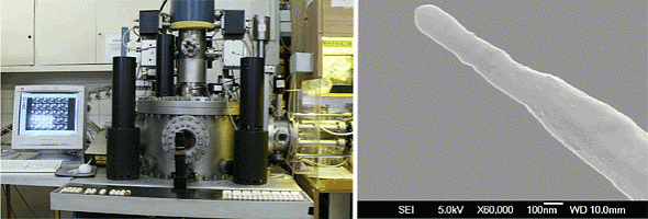
E-beam pattern generator (left), cathode – tip detail from SEM (right)
E-Beam lithography technology
A required image is enregistered into the thin polymer layer (positive or
negative electron resist) by the beam of electrons. The resist-layer mask is
created by the development of the exposed patterns. The substrate surface (or
the working layer previously deposited on the substrate – either a metallic
or a dielectric one) is modified through the resist openings.
EBL originated samples and applications:
- Dimension standard structure.
- Masters for nano imprint lithography (NIL).
- Glass masks for optical and UV lithography.
- Direct write lithography.
- Micro and nano relief characterization by atomic force microscopy (AFM).
Selected R&D result used by industrial partners:
- A few samples of metrology dimension standards for both optical and e beam microscopy were delivered to several customers. The precision of the samples is derived from the laser-interferometer calibrated exposure field of the e beam pattern generator. The samples are basically composed of the scale, rectangular gratings with different periods and a set of geometrical shapes with a description.
Contact:
Dr. František Matějka
e-mail: matejka@isibrno.cz
phone: +420 541 514 221
Ing. Milan Matějka
e-mail: mmatejka@isibrno.cz
phone: +420 541 514 344
Dr. Vladimir Kolařík
e-mail: kolariq@isibrno.cz
phone: +420 541 514 336
Detailed information: http://www.isibrno.cz/teams/EBL
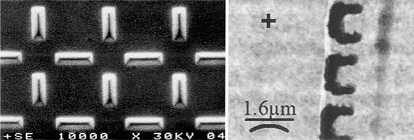
Dimension standard structure (detail) grating period 5 µm (left), self-switching diode device (AFM) (right)
Optical diffractive structures
The resolution of the e-beam writer for the delineating of gratings with a period below 1 micron which is close to the visible light range (400–700 nm). With a relatively high writing speed, optical diffractive structures of several cm2 can be prepared.
Due to the flexibility of the technology a variable set of diffraction
gratings as well as their combination within one sample is possible e.g.
reflection or transmission gratings, phase or amplitude gratings, regular
(lines, crosses, circles) and irregular structures (Fournier, Fresnel), binary
and multilevel profile and so on.
EBL applications:
- Phase diffractive optical elements (phase DOE’s) – methodology and technology of structure preparation.
- Industrial applications of EBL in the field of computer generated holograms (CGH), i.e. synthetic holograms patterned by the direct e beam writing process (groove by groove) as opposed to the laser interference method.
- Optical diffractive Fresnel lenses.
Selected R&D result used by industrial partner:
- A few dozen samples with large-area holographic structures (prepared in the polymer electron resist layer) were delivered according to the customer’s technical specifications.
Contact:
Dr. Vladimír Kolařík
e-mail: kolariq@isibrno.cz
phone: +420 541 514 336
Detailed information: http://www.isibrno.cz/teams/EBL
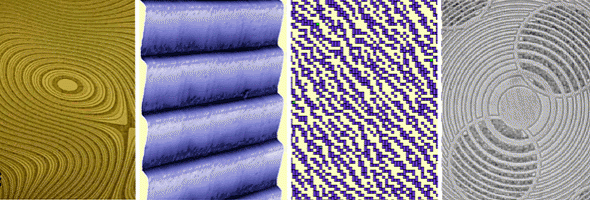
Detail of a general diffractive multilevel structure – optical microscope 200× (left), relief of a regular asymmetric diffractive grating pitch 4 µm – deepness 0.5 µm (middle – left), CHG structure – layout simulation (middle – right), zonal structrue with a diffuser (right)