Electron microscopy
Electron microscopy is a globally used technique for the examination of matter with an extremely broad scope of applications in life, materials and even social sciences. The Laboratory of Electron Microscopy (LEM) has a great deal of experience in the development and use of instrumentation as well as in electron microscopy methodology; at present it offers several unique methods of imaging and analysis of solid surfaces at high spatial resolution.
- The ultimate spatial resolution is achievable by means of the cold field emission source of electrons available in the JEOL JSM 6700F scanning electron microscope with verified resolution of 1 nm at the electron energy of 15 keV. The microscope is equipped with the energy dispersive analyser of X-rays Oxford INCA Energy 350 for chemical microanalysis.
- Methodology for the very low energy scanning electron microscopy has been developed at ISI and the corresponding attachments are installed on several microscopes in LEM. The method enables the preservation of image resolution down to arbitrarily low energy, which is not possible in commercially available instruments. At very low energies plenty of novel contrast mechanisms reveal electronic and crystallinic structures of the sample.
- Environmental scanning electron microscopy (ESEM) enables the study of samples of living substances and materials under elevated pressure of surrounding gas up to 3000 Pa. In this environment charging of nonconductive samples is avoided and even wet matter can be protected against drying . The ESEM instruments also work under the standard high vacuum conditions.
- Electron microscopy under ultrahigh vacuum conditions of 10–8 Pa enables one to study atomically clean surfaces that can be cleaned in-situ with ion beam bombardment. The device offers excellent conditions for the low energy microscopy.
- LEM has available standard preparation techniques such as sputtering and evaporation of surface coatings, ion beam thinning, exact cutting. Complementary light optical imaging is possible with the confocal microscope Olympus LEXT 3100.
High resolution scanning electron microscopy and X-ray microanalysis
The high resolution scanning electron microscopy applications are met in
nearly all scientific branches. In combination with the X-ray microanalysis it
provides information about the surface topography of a sample together with its
local quantitative composition as regards chemical elements.
Advantages and application examples:
- Imaging with four different detectors provides complex information about the sample.
- Surface observation at very low energies down to about 20 eV at high resolution.
- Secondary electrons informing about the surface topography are detected with two complementary detectors.
- Backscattered electrons are also detected with two different detectors, with a possibility of acquiring the complete emission including the high angle scattered electrons not available in conventional instruments.
- Resolution of 1 nm, achieved without any aberration corrector, is fully sufficient for the examination of virtually all micro- and nano- structures.
- Quantitative chemical composition in combination with the high resolution imaging leaves very little unknown about any sample.
- Low magnification mode enables one to very comfortably seek out the area of interest.
Contact:
Filip Mika, M. Eng., Ph.D.
e-mail: fumici@isibrno.cz
phone: +420 541 514 298
Detailed information: http://www.isibrno.cz
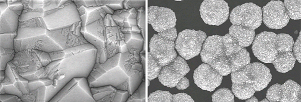
Surface of a synthesized diamond coating (left), clusters of micrometer sized diamond grains (right)
Scanning microscopy with slow electrons
Scanning microscopy with slow electrons utilizes the principle of so-called
cathode lens retarding of the electron beam just in front of the sample surface.
In this way the electron beam is formed and focused at high energy and so the
illuminating spot governing the image resolution can be very small for all
energies of electrons between 15 keV and 1 eV. The unique detector solution
provides very high efficiency of signal collection and high amplification even
at the lowest energies.
Advantages and application examples:
- Diminished volume of the interaction of slow electrons inside the sample and thus improved resolution for real samples and enhanced surface sensitivity.
- Increased signal of secondary electrons improving the signal-to-noise ratio in the image signal.
- Imaging of nonconductive samples at optimum energy of electrons not causing local charges even under high vacuum
- In depth analysis of samples via energy based tomography.
- Imaging of dopants in semiconductors and measurement of their density.
- Tailoring the electron energy to maximum contrast between different materials.
- Acquisition of signal electrons backscattered under large angles from the optical axis, bearing enhanced crystallinity contrast.
Contact:
Ilona Müllerová, M.Eng., Ph.D., D.Sc.
e-mail: ilona@isibrno.cz
phone: +420 541 514 300
Detailed information: http://www.isibrno.cz
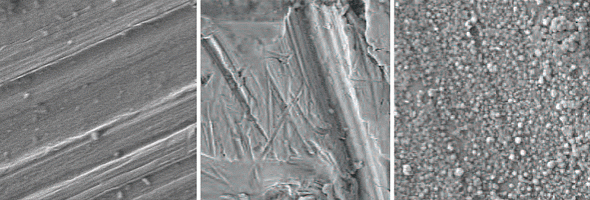
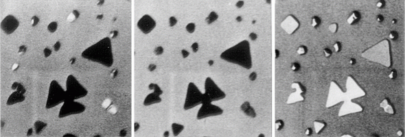
Surface of writing paper in its original nonconductive status (left), the optimum electron energy for suppressed charging (middle, right)
Environmental scanning electron microscopy and detection systems
The environmental scanning electron microscopy (ESEM) is a modern solution for the observation of any type of nonconductive objects without the necessity of coating with a metallic or carbon layer. In addition, wet samples of animate or inanimate origin can be preserved and observed close to their natural status.
If the gas pressure in the specimen chamber of ESEM is higher than about
200 Pa, the primary and signal electrons collide with gas molecules in the
vicinity of the sample and ions generated in this way compensate for the
charging of the specimen by incident electrons. If the pressure of gas, or
rather water vapours, in the specimen chamber is higher than 611 Pa (at 0°C),
wet objects do not dry up and remain observable in their original non-collapsed
shape.
The ESEM can be used to study:
- the surface structure of conducting and non-conducting natural animate and inanimate samples;
- wet samples and samples near the phase transition (condensation, evaporation, melting, solidification, etc.);
- specimens in conditions of mechanical and thermal strain in the vacuum or in a gas of optional humidity;
- material, topographic or voltage contrast enabling one to observe electric charge accumulation and distribution e.g. on transistor gates;
- reactions of various chemical substances in the specimen chamber;
- aggressive chemical substances, e.g. battery mass;
- various types of specimens in conditions close to atmospheric pressure.
Selected applications of ESEM and research results obtained in cooperation with industrial partners:
- Study of dozens of selected materials before and after corrosion by chemical substances, specification of the resistance and lifetime of examined materials and assessment of the changes of their mechanical properties due to corrosion.
- Study of inner surfaces of several types of vascular catheters in order to assess the surface relief from the point of view of danger of the embolism.
- Study of the surface of working electrodes of electrochemical sensors oriented at mapping the surface topography structure, measurement of its real and geometric surface area and subsequent optimization of the production process and launching of a new type of electrochemical sensor.
- Study of the surface structure of solar cells to map the effects of laser beam machining on cell properties.
- In cooperation with a medical institution an extensive study has been performed on the effects of different techniques for the removal of tartar from human teeth.
Contact:
Ing. et Ing. Vilém Neděla, Ph.D.
e-mail: vilem@isibrno.cz
phone: +420 541 514 333
Detailed information: http://www.isibrno.cz
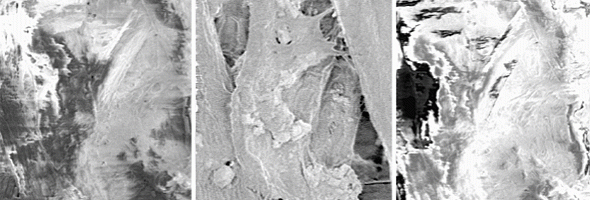
Uncorroded surface of Tantalum (left), Tantalum surface corroded in H2SO4 (middle), Tantalum surface corroded in KOH (right)
Electron microscopy under ultrahigh vacuum conditions
Microscopy and the analysis of very clean surfaces under ultrahigh vacuum conditions represent an irreplaceable tool for contemporary and, in particular, new nanotechnologies. ISI has built its own version of the ultrahigh vacuum scanning electron microscope for examination of atomically clean and defined or even in-situ prepared surfaces of solids. The microscope has an operational vacuum of 10–8 Pa thanks to its complete bakeability, but samples are readily exchanged via vacuum airlock. The device is composed of three vacuum chambers: the observation chamber, preparation chamber and airlock. In the observation chamber the electron optical column enables one to work at all electron energies down to fractions of eV or even to acquire the mirror image of the sample. Detectors available include acquisition of the complete backscattered emission at all energies, secondary electron emission, transmitted electron emission and detection and analysis of gases released by electrons. The device will soon be equipped with an energy analyzer of Auger electrons. In the preparation chamber devices are available for ion beam cleaning and sputtering of the sample surface and for evaporation of up to three different materials.
ISI plans to purchase a photoemission electron microscope combined with a
direct imaging low energy electron microscope for complex examination of clean
crystalline surfaces of all kinds.
Advantages and application examples:
- The unique sample stage/detector assembly enables the adjustment of the device for perfect performance at arbitrarily low energies.
- The electric field above the sample collects the complete emission and hence provides full available information.
- A very high collection efficiency of signal detection increases the signal-to-noise ratio in images and speeds up data acquisition.
- At very low energies novel contrast mechanisms appear in micrographs, revealing the electronic and crystalline structure in addition to the conventional topographic and material contrast.
- Small interaction volume substantially improves the resolution of details immersed below or protruding above the surface and the surface sensitivity in general.
- Grains in polycrystals become visible in high contrast, including subgrains, twins, etc., with the possibility of identifying their orientation.
- Internal stress in polycrystalline materials is mapped in high contrast and resolution.
- The doped areas in semiconductors can be quantitatively examined and critical dimensions measured exactly.
- At very low energies the radiation damage of extremely sensitive samples ceases.
- Thanks to their longer wavelength very slow electrons produce diffraction and interference phenomena, providing novel tools for the examination of nanostructures.
Contact:
Miloš Hovorka, M.Sc.
e-mail: hovorka@isibrno.cz
phone: +420 541 514 259
Detailed information: http://www.isibrno.cz
Atomically flat two-dimensional crystals of lead on the silicon surface, imaged by means of the dark-field diffraction contrast